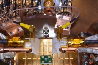
 Capacitance-voltage (C-V) measurements are widely used by device and material researchers to characterize fundamental properties of new devices—typically under ambient conditions. A new app note demonstrates Lake Shore’s approach to ensuring high-quality, wafer-level C-V measurements in a cryogenic probing environment. This new approach enables variable-temperature, wafer-level C-V measurements which could be used, for example, to measure temperature-dependent carrier concentrations in processed devices or better elucidate defects and trap states in a device under test (DUT).
The app note discusses temperature-dependent C-V measurements performed in Lake Shore TTPX, CPX-VF, and CRX-4K probe stations equipped with special dual-connector probes. These probes are supplied in a measurement kit that also includes the cabling and adapters necessary to establish a shielded, two-terminal (S-2T) configuration. The S-2T configuration is achieved by linking the coaxial shields inside the prober as close as possible to the DUT. The linkage is important because it creates a current return path, which cancels the magnetic flux generated by the measurement. Without this return path current, the unmitigated flux would cause an increase in the residual cable inductance and can vary with the placement of the probes—reducing the overall accuracy of the capacitance measurement.
