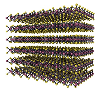
Since isolated graphene was first reported in 2004, a lot of two-dimensional (2D) material research has focused on developing the strong, single-atom-thick material for end use in novel electronic and optoelectronic designs, including more flexible replacements for silicon-based circuits. More recently, however, a considerable amount of study has been with 2D graphene-analogs, such as phosphorene, as well as 2D forms of transition metal dichalcogenides (TMDs or TMDCs)—for example, molybdenum disulfide (MoS2). The main reason: many of these next-generation 2D materials inherently feature a band gap (graphene has no such gap, which limits its utility in transistor designs). Because some of these novel 2D materials exhibit semiconducting properties with highly tunable bandgaps, they could open the door to a wider range of electronic, photovoltaic, and energy storage applications, particularly new field-effect transistor (FET) devices. Others exhibit superconductive states at low temperatures (for instance, single-layer NbSe2 has been found to be a “true 2D superconductor” in its isolated, 2D form without the need for a special substrate). Researchers are also experimenting with hybrid 2D Van der Waals heterostructures comprising both graphene and TMD materials fabricated via chemical vapor deposition (CVD), atomic layer deposition (ALD), and other synthesis methodologies.
By observing the number of papers being published, we have seen an increasing number of researchers who are using Lake Shore cryogenic probe stations in their 2D electronic materials-related work. In addition to MoS2 transistor-related research, our stations have been used to study temperature-dependent transport behaviors within multilayer indium selenide (InSe) FETs, as well as niobium diselenide (NbSe2) nanostructures with CVD-synthesized crystalline structures.
Lake Shore cryogenic probe stations offer a versatile platform for probing and characterizing the electro-optical and magneto-transport properties of TMD devices patterned on wafers up to 51 mm (2 in) in diameter, including temperature-dependent, gated I-V characteristics. Like graphene, the atomically-thin TMD structures can be significantly affected by surface contamination caused by atmospheric exposure. Conducting transport measurements within the vacuum conditions (as low as 10-8 Torr) of the probe station helps minimize the risk of this occurring. Sample contamination can be further minimized with the addition of a load-lock with suitcase. The load-lock option can be added to several probe station models and allows the researcher to move a device from glove box to electrical test in a controlled atmosphere.
Although TMD and graphene-analog materials are commonly investigated at room temperature, temperature-dependent investigation of carrier mobility can reveal insights into phonon scattering as well as defect concentration, movement, and location. Moreover, with sample stage temperatures as low as 1.6 K, Lake Shore cryogenic probe stations are ideal platforms for on-wafer characterization of 2D superconducting devices—particularly at microwave frequencies.
For help choosing a probe station, as well as a material characterization system such as a Hall effect measurement system (for measuring Hall mobility of TMDs as a function of temperature and applied gate bias), please contact us.
