
Van der Waals (vdW) 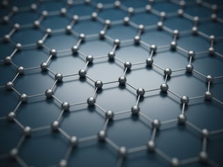 heterostructures offer researchers an unprecedented opportunity to tailor device architectures and derive new physical properties through atomic-scale layering of two-dimensional (2D) materials. These so-called van der Waals materials (such as graphene, hexagonal boron nitride, and molybdenum disulfide) are characterized by strong interlayer bonds with weak intralayer (vdW) forces. By combining such materials, scientists “are anticipating observing novel lattice structures and electronic properties which cannot be achieved in conventional bulk materials.”1 In the last couple of years, we have observed from published papers how Lake Shore products have aided in this type of work, mainly for the characterization of transport mechanisms of the engineered heterostructures.
The combination of low current leakage with environmental control found in our vacuum probe stations provide distinct advantages for this type of 2D material research. As many vdW materials are chemically unstable in air, electronic characterization of these research-grade devices must be carried out in a vacuum environment. Additionally, the stations can be used for the study of certain multilayered devices at different vacuum pressures, providing insights into the influence of, for instance, absorbed oxygen and water on the charge transport properties.2
Recent papers detailing such 2D heterostructure investigations include:
- Researchers from China’s National Center for Nanoscience & Technology and the University of Chinese Academy of Sciences developing semi-vertical field effect transistors (SVFETs) with more photo-responsive characteristics. For this, they fabricated molybdenum ditelluride (MoTe2)/molybdenum disulfide (MoS2) transistors, where the “lateral MoTe2 parts act as channels and the vdWs underneath the electrodes form vertical transport paths.” For device characterization, electrical transport measurements were performed in a Lake Shore TTPX probe station under vacuum.
- Tsinghua University and Beijing University of Technology researchers who fabricated a CNT/tungsten diselenide (WSe2)/graphene heterostructure for potential use as high-performance photodetectors. In this application, a 1D CNT was added to a stack of 2D materials, with our CRX-4K probe station used for in-vacuum, electrical measurements of the mixed-dimensional vdW heterostructure.
- A team of researchers from Russia and Austria who fabricated molybdenum disulfide (MoS2)/epitaxial fluorite (CaF2) FETs as part of work developing high-quality gate insulators compatible with 2D technologies. They extended the stacking properties of 2D heterostructures to the CaF2 layers, forming a “quasi” vdW interface with the MoS2 semiconductors, and in the process, achieved “a breakthrough towards enabling ultra-scaled dielectric layers for next-generation 2D nanoelectronics.” For this research, a Lake Shore probe station was used to measure samples under ∼5 × 10⁻⁶ torr in vacuum and in complete darkness.
- In another MoS2 related paper, a team led by researchers from New York University and Columbia University reported on fabricating metal contacts on 2D materials with high reproducibility. The team specifically fabricated MoS2 FETs, finding “linear I-V curves even at low temperatures, record-low Schottky barrier heights (~0 mV), record high on/off ratios (109 – 1010) and exceptionally low subthreshold swing (64 mV per decade).” For characterizing the exfoliated samples, they used a Lake Shore probe station at 10−5 torr under vacuum.
Aside from probe stations, we also offer highly sensitive VSMs for characterizing vdW structures containing magnetic materials and nanoparticles, as well as the new MeasureReady™ M91 FastHall™ measurement controller, which can accelerate Hall mobility measurements of 2D semiconducting materials whether used on its own or in conjunction with a probe station equipped with an electromagnetic or superconducting magnet.
1 Joint Research on Novel Physical Properties and Functionalities of Emerging 2D Materials and van der Waals Heterostructures, A3 Foresight Program
2 “Conversion of Multi-layered MoTe2 Transistor Between P-Type and N-Type and Their Use in Inverter,” Nanoscale Research Letters, v. 13, 2018, DOI: 10.1186/s11671-018-2721-0